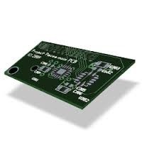

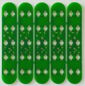
PCB Copy Design Service
12 Per Square Centimeter
We are engaged in offering PCB Copy Design Service.Features: Improved quick-track fiber-tear properties Use of stronger fiberglass Better chemical resistance Specifications: Characterized by Silk screen, Solder Mask and HAL (SMOBC) Made up of Fr4 and CM1 material Available in CU thickness of 17.5 and 35 micron, with the material thickness of 0.8mm, 1.6 mm and 2.4 mm. MOQ 1 Sq.cm
pcb designing services
4,000 Per Piece
PCB designing services are offered by many but only days or are known to offer it exceptionally well. Their expertise harmonises with innovation and the profession, a team of skilled engineers known for crafting, intricate and efficient printed circuit board (PCB) designs. They elevate electronic product development to the next level with their skill and proficiency. Their utilisation of advanced tools and adeptly navigating through complex design challenges helps them build something out of the box while adhering to stringent quality standards. With their proven track record and huge client base, you can trust their proficiency in delivering tailored PCB layouts that seamlessly optimise functionality. Their services also enhance performance and streamline production processes. For your business, all you need to have is their PCB designing services and there will be a long way for you to go without any bottlenecks.
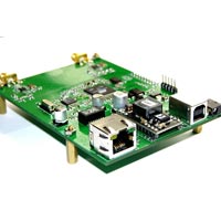
Looking for PCB Design Service Providers
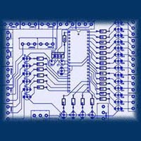
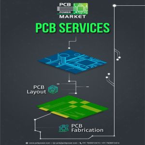
Double Layer PCB Designing Services
Get Price Quote
Aptel Circuit is pleased to introduce itself as a reputable provider of Double Layer PCB Designing Services in Surat, Gujarat. We have a lot of experience in PCB Design Services, which we do underneath the direct supervision of our professionals.Schematic capturing, PCB layout, plus board procurement are all part of our PCB Design Services. Our specialists provide these services, and they have a lot of experience in this field.As a result of this feature, you may rely on us to provide PCB Design Services without any reservations. We are customer-focused and provide high-quality multilayered high-speed PCB designs that take real-world production and test needs into account.

pcb design service
Get Price Quote
At Advanced Circuit, our PCB design service is aimed at assisting our customers quickly get to the market, given the vast specialization we have in PCB designing for better manufacturability and efficiency. Based in Surat, we started operating in 2018 and we take pride in holding expertise in offering both upgrades to your existing PCB and creating fresh PCB designs right from the start. High-Quality PCB Designing Solutions Our team of designers are always ready to discuss your project requirements, as we aren’t only licensed but we are also known to take the help of only specialized tools for designing purposes. We have all that it takes to cater to the highest industrial standards. Get in touch with us to know more about our services.
pcb design service
Get Price Quote
PCB Designing
Get Price Quote
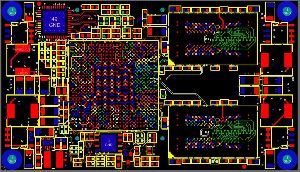
Team with highly skilled pcb layout engineers. The stringent process, continual training programs on current technologies are the keys for the success of the company. The experience acquired from handling highly complex pcb designs for cutting-edge technologies spread across major industry. Our established design credentials combined with world class prototyping facilities makes the logical design into a working printed circuit board in the quickest turnaround time. · over 200 complex designs completed. · expertise in high speed digital, mixed signal, analog & power boards. · innovative design methods in fine pitch micro bga designs. · handled upto 0.4mm bga pitch designs with 2 mil 2mil trackspacings. · integrating mechanical & electrical cad data for assembly verification. · board level, system level si, pi, emiemc & thermal analysis. · dc drop analysis in power supply rails due to copper losses. · over the years we have developed custom programs and scripts to gain efficiencies, improve quality and augment the current design tools.
pcb design service
Get Price Quote
1 Piece(s) (MOQ)
we are pcb designer's from bengaluru, Karnatka, India, we are experts in pcb Designing and development.

pcb designing services
Get Price Quote
For all those who are looking out for the most trusted PCB Designing Services, can contact us. We offer the best deal and ideal solutions.
pcb design service
Get Price Quote
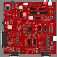
HARDWARE ENGINEERING PCB Design and Layout • Schematic • Complex PCB Design • Low Power Design • MECHANICAL ENGINEERING Product Design • 3D Modelling • Industrial & Ruggedized Design • Thermal Analysis • Certifications FPGA DEVELOPMENT • FPGA Design • RTL Coding and Verification • FPGA POC • Emulators and Prototyping FIRMWARE ENGINEERING • Firmware, Middleware • Device Driver • BSP • OS Porting & Customization • Embedded Application TESTING & CERTIFICATIONS • Agile • Testing & Validation • Interoperability Testing • QA Automation • Certification
PCB Design Fabrication Lab
Get Price Quote
1 Piece(s) (MOQ)
pcb design service
Get Price Quote
100 hours (MOQ)
Ø High frequency AC-DC, DC-DC converters design using Buck, Boost, Fly back, Push pull, half Bridge and Full Bridge topologies Ø Inverters, online UPS design for power backup applications Ø Li-IonPoly and Lead acid battery chargers design Ø Power architecture and power management solutions

pcb design service
500 Per Piece
XxiLLENCE Inc. is providing High Speed PCB Design Engineering Services from its incorporation in the year 2007. We are situated in Bangalore, the silicon city of India, and offer our complete PCB Design Engineering Services and Solutions to R&D Engineering Sectors in India and aboard at cost effective economical rate. Our Engineering team have achieved client's satisfaction in the PCB Design Engineering Sector through continuous dedication and focus towards the requirement and the critical aspects of each and every project with strict adherence to the guidelines, standards and schedule.
pcb design service
Get Price Quote
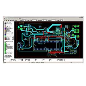
Tips provide pcb layout design services in worldwide used designing software. Pcb layout design services: 1. make outline as per customer requirement. 2. convert schematic to layout design. 3. put mounting hole as per customer requirement. 4. make cutout as per customer requirement. 5. make slot drill as per customer requirement. 6. make drill drawing. 7. make customer specific arraypanelization. 8. design single ended differential trace layout. 9. taken gerber 274x or other format output of design. 10. taken nc drill output of drill. 11. make fabrication drawing.
electronic circuit board design
Get Price Quote
100 Set (MOQ)
Pcb Design Services
Get Price Quote
We take pride in introducing ourselves as a reputed provider of PCB Design Services in Ghaziabad. We hold immense expertise in undertaking PCB Design Services under the strict supervision of our experts. Our PCB Design Services include designing of schematic capture, PCB layout and board procurement. These services are rendered by our professionals who hold immense experience in this domain. Because of this factor, one can obtain PCB Design Services from us without having any iota of doubt.
PCB Designing
Get Price Quote
We are the leading organization to offer our precious clients an optimum quality PCB Design Services. This service is carried out under the strict supervision of our experts using the best grade tools and advanced techniques. Our skilled professionals ensure the clients that the service, provided by us is highly reliable and executed in an excellent manner. The offered service is performed within a stipulated time-frame. Furthermore, this service can be availed by our clients at budget-friendly prices. We are one of the best PCB design companies that can drastically reduce the cost of circuit board design by employing our global design center effectively in projects. Our designers will ensure that cost of manufacturing and assembling is optimized by using the right design techniques. Our team closely works with the clients to determine their exact needs and provide what is required without adding too much into the design. We believe it would only complicate the process. PCB layout helps to initiate a reliable outsourcing relationship with those involved in the process. Most of the PCB design companies employ local contractors who have the adequate skill set to work with another party to get the PCB design made. Engaging hardware engineers to develop and draft the schematics and PCB layout services usually slows down the process and creates congestion for the R&D team. Likewise, managing several designs at once can be difficult for most of the PCB layout teams.
Hardware & PCB Designing Services
Get Price Quote
New-age products demand extreme reliability at the lowest costs to be achieved in the shortest possible timeline. We have a group of experts in hardware design and development who undertake the complete ownership of hardware product design. Hardware Architecture Planning Schematic Capture Board Design BOM Generation

PCB Design
Get Price Quote
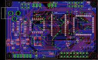
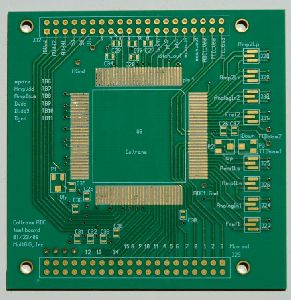
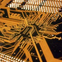
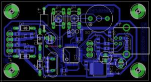
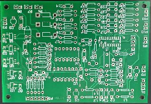
A basic PCB consists of a flat sheet of insulating material and a layer of copper foil, laminated to the substrate. Chemical etching divides the copper into separate conducting lines called tracks or circuit traces, pads for connections, vias to pass connections between layers of copper, and features such as solid conductive areas for electromagnetic shielding or other purposes. The tracks function as wires fixed in place, and are insulated from each other by air and the board substrate material. The surface of a PCB may have a coating that protects the copper from corrosion and reduces the chances of solder shorts between traces or undesired electrical contact with stray bare wires. For its function in helping to prevent solder shorts, the coating is called solder resist or solder mask.
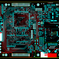
PCB Structure Design Services
Get Price Quote
Aero Track Circuit is a Surat (Gujarat, India) based company, which is involved in providing top-class PCB structure design services to the clients. With the support of a team of deft PCB structure design experts, it has become possible for us to maintain the quality of layout results that directly affect the effectiveness of the wiring. Working in the service sector for more than two decades, we have been able to gain a huge clientele in the city by offering top-notch services at affordable charges.
Pcb Design Services
Get Price Quote
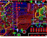
Argus have established standards for acceptance and delivery which results in faster turnaround time with least error. Our PCB Design environment uses best in industry tools like Mentor Graphics and Cadence for design capture, PCB layout and design analysis. We are customer centric and deliver high quality multi layer high-speed PCB designs, taking into consideration of real-world manufacturing and test requirements. Our PCB design services includes: High degree of Expertise in High speed PCB designs. High speed digital, Analog, mixed digitalanalog, RF designs. High Layer count (30 layers), Ultra High density designs. Impedance controlled Designs with delay matching, Stack-up and material selection. Standards Compliant (IPC, UL, MIL, DO-254) designs as per customer specifications. High speed interconnects : 2.5Gbps. Multiple Fine pitch BGA (0.5mm) of high pin count(1136). Designs with Micro Vias, Blind Vias, Buried Vias and backdrill. Motherboards, Single Board computers, High speed Serial Backplanes, Telecom Backplane. ASIC Test Boards, Load Boards, Probe Cards, Burn-in Boards, sockets, Package Design. Pre-Route and post-route Signal Integrity Analysis, IBIS Model Creation. Cross talk analysis, Timing analysis, EMI analysis, Power Integrity analysis.
PCB Designing
Get Price Quote
We are a name to reckon when it comes to reliable PCB Designing solutions in Vadodara. We have all the resources for providing PCB Designing service as per the enterprise requirement. In addition to PCB Designing, we also offer design services for the global PCB market.Our Printed Circuit Board (PCB) Design capability includes : System Architecture Design Schematic Design & Verification Digital/ Analogue / RF and mixed signal PCBs Junction temperature sensing and thermal management Power Optimized Battery Operated Designs High Density, Thermally Efficient Designs Signal Integrity Simulation and Verification Board Design Up to 7 layers PCB Layout Design Layout /Routing analysis and optimization Gerber Generation and Verification Hardware Design Validation Library Creation and Management Production and Testing Services PCB Fabrication with Third Party PCB Assembly with Third Party Manual Testing
Pcb Design Services
Get Price Quote
We are providing pcb design services. As we provides our clients best type of pcb designing layout as per the specifactions, drawing and clients requirement. We provide pcb/electronics design, schematic, layoyt and cam services etc. Which is widely used in electronics industries.our designing cantains software programming, micro-controlling, embedded system, analog & digital electronics etc. Our pcb development and pcb designing is fast and punctual with excellent work and super finishing.
PCB Design
Get Price Quote
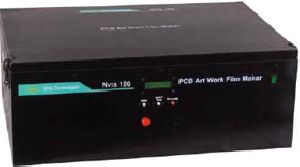
Nvis PCB LAB is a complete solution for designing PCB. This solution includes all the necessary machines and chemicals which are used in the PCB development process. The PCB artwork film maker is used as a contact printer for creating design films from the PCB Layout. The artwork table is used for manually designing the films and for correcting or changing the existing films. The shearing machine is used for cutting the PCB according to film size. The photoresist dip coating machine is used for coating photoresist on the PCB Laminate. After photoresist coating, the PCB and films are placed in UV exposure machine for exposing. After exposing the development tank is used to remove unused photoresist. The dye tank is used for highlighting the design on the PCB. The etching machine is used for removing unused copper from the PCB. The drilling machine is used for making the holes in the PCB. The PCB design kit is provided which include tapes, stencils and other accessories used for designing the PCB.
Printed Circuit Board Designing
Get Price Quote
Contact us, if you are looking for Printed Circuit Board Designing Service in Delhi. We hold all the expertise and mechanism for designing and developing the best-in-class PCB. Based on latest technology, our Printed Circuit Boards comply with the defined parameters of the industry. The entire production process of these Printed Circuit Boards is executed under the supervision of our professional team members. The Printed Circuit Board Designing is done only by experts to meet the applications of various industries. Along with Printed Circuit Board Designing, we provide soldering solutions as well as complete PCB layout. We also entertain prototype and small quantity inquiries.
pcb design service
1 Per Piece
pcb design service
Pcb Design Services
Get Price Quote
Pcb Design Services, IoT Product Development, embedded solution
pcb design service
Get Price Quote
pcb design service, CRUSHER CONVEYOR METAL DETECTOR

pcb design service
5,000 Per Piece
price is as per requirement based on their productsservice details:- the prices which are mentioned over here is the starting prices they may vary as per the requirement pcb design with an increasing demand for products with the latest technologies, it is a challenge to keep pace with the upcoming technologies while retaining resources to maintain legacy designs. in addition to the growing competition amongst industries, the challenges posed by evolving technologies, innovation cycles and product re-engineering has driven engineering companies to focus on manufacturing process optimization and reducing design costs. an expert pcb fabrication is a key building block for all electronic products. we as a single source ems provider, are committed to providing better manufacturability and reliability. with our strategic partnership with world”s leading pcb fabricators, we are set to make production cost-effective with high quality. indra insignia broad range of pcb fabrication options include: pcb fabrication up to 60 layers board thickness from 0.015” to 0.500” copper weight from 12 microns (3/8 oz.) to 343 microns (10 oz.) panel sizes up to 31” x 52” large form factor and high-aspect-ratio backplanes embedded passives (zbc™, buried capacitance®, annular buried resistance technologies) high-performance materials and composites signal-integrity modeling high-speed 10gps leadership through innovative engineering fabrication of rigid-flex-rigid boards
pcb design service
Get Price Quote
pcb design service, Printed Circuit Board, PCB Assembly Services
multilayer PCB design service
Get Price Quote
team with highly skilled pcb layout engineers. The stringent process, continual training programs on current technologies are the keys for the success of the company. The experience acquired from handling highly complex pcb designs for cutting-edge technologies spread across major industry. our established design credentials combined with world class prototyping facilities makes the logical design into a working printed circuit board in the quickest turnaround time. · over 200 complex designs completed. · expertise in high speed digital, mixed signal, analog & power boards. · innovative design methods in fine pitch micro bga designs. · handled upto 0.4mm bga pitch designs with 2 mil/ 2mil track/spacings. · integrating mechanical & electrical cad data for assembly verification. · board level, system-level si, pi, emi/emc & thermal analysis. · dc drop analysis in power supply rails due to copper losses. · over the years we have developed custom programs and scripts to gain efficiencies, improve quality and augment the current design tools.