XILINK USB DONGLE
LOGIC ANALYSER AND PATTERN GENERATOR
UNIVERSAL PROGRAMMER
Why Programmer…
The Programmer is an important tool in developmental activities. The tool helps you to program various devices as per your requirement.
There are various models depending upon the requirement of the developer.
Various adaptors are also available for various kinds of packages.
SPRING BOARD WITH 16 PIN IC BASE - DUAL LINE
SPRING BOARD WITH 16 PIN IC BASE - SINGLE LINE
SPRING BOARD WITH 8 PIN IC BASE - DUAL LINE
SPRING BOARD WITH 8 PIN IC BASE - SINGLE LINE
GENERAL PURPOSE SPRING BOARD WITH 32 SPRINGS
SPRING BOARD WITH TWO 16 PIN ZIF SOCKETS AND 64 SPRINGS
CUSTOMISED SPRING BOARDS CAN ALSO BE DONE
MICROCONTROLLER BASED
VARIABLE DC OFFSET CONTROL
VARIABLE AMPLITUDE CONTROL
BUILT-IN 5 DIGIT INT AND EXT COUNTER DISPLAY
2-IN-1 FUNCTION – FREQUENCY COUNTER AND GENERATOR
50 OHMS AND 600 OHMS OUTPUT IMPEDENCE SELECTABLE
VARIABLE OUTPUT LEVEL CONTROL WITH 10db,20db and 40db ATTENUATOR RANGES
VERSATILE WAVEFORMS OF SINE,SQUARE,TRIANGULAR AND PULSE WITH VARIABLE DUTY CYCLE
This unit is Microcontroller based controller circuit to accurately generate pulses to energize the stepper motor winding in the desired sequence. Power Transistor based driver circuit to drive the stepper motor. 5 Seven segment display to set and display the parameters. From this controller we can set the speed of the stepper motor in RPM, set the number of steps the motor can move. We can set the direction of rotation – forward and reverse direction. We can also set half step and full step mode.
This unit is Microcontroller based controller circuit to accurately generate pulses to energize the stepper motor winding in the desired sequence. Power Transistor based driver circuit to drive the stepper motor. 5 Seven segment display to set and display the parameters. From this controller we can set the speed of the stepper motor in RPM, set the number of steps the motor can move. We can set the direction of rotation – forward and reverse direction. We can also set half step and full step mode.
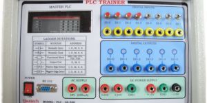
MAIN UNIT: Microprocessor based PLC System with built in 8 Digital input line, with RS232 Serial Interface of Industrial grade PLC will be used. The system comes with Ladder programming and communication software compatible with IBM PC. All the inputs and outputs are brought out to the panels for the ease of studying various Static application panels and also Sample Ladder programs are supplied for better understanding of PLC. The Panel is built with necessary Power supply required for the PLC and the Simulation Panels. The system can be used for any control applications, which come across in Industrial Environment by writing Logic program as per requirement.
MAIN UNIT: Microprocessor based PLC System with built in 8 Digital input line, with RS232 Serial Interface of Industrial grade PLC will be used. The system comes with Ladder programming and communication software compatible with IBM PC. All the inputs and outputs are brought out to the panels for the ease of studying various Static application panels and also Sample Ladder programs are supplied for better understanding of PLC. The Panel is built with necessary Power supply required for the PLC and the Simulation Panels. The system can be used for any control applications, which come across in Industrial Environment by writing Logic program as per requirement.
PCI-07A 24 LINES DIGITAL IO CARD WITH TIMER
The card has 24 digital IO lines using PPI 8255. The 8255 lines are terminated in a 26 pin FRC header
PCI - 08 16 CHANNEL RELAY OUTPUT CARD
This is a 16 Channel Relay Output card
Reed Relay Type SPST
Contact Rating 28V DC500 mA switching current
Operate Time 1 msecs
Release Time 1 msecs. LED's for relay state indication. Single Software command to deenergise all the relays
Output connection Terminations are brought out through Multi-core cable using D-type connector to a cable box which has requisite Termination Blocks for external connection
The ALS_PCI_05 is a general purpose PCI Prototyping board with an onboard CPLD that generates required signals that permit the user to perform single cycle read write from to the users hardware, in the pass through mode.
The Add-On bus signals are also routed to a set of four external application burg strip headers. These headers can provide the designer a quick interconnection between the Add-On bus signals and test hardware in the prototyping area. The EPLD is programmed to provide sufficient number of chip selects which can be used for Add-On hardware. Read and Write signals are separately provided.
Sufficient number of ground and supply pads to the proto-typing area
Three groups of chip selects to choose from 8, 16 and 32 bit region
Provision to generate additional chip selects using available lower order demultiplexed address lines
All the Add-On signals are terminated on burg strip headers
Additional 25-pin connector provided at the card edge to terminate signals from the development area
Ready software to perform Add-On IO read and write operation from the PC end in the pass through mode
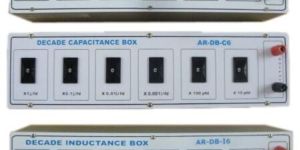
ACCURACY +-0.5% + 1 DIGIT
RANGE
L 0-2000H
C 0-2000UFD
R 0-20 MΩ
RESOLUTION
0.1µHPFΩ
DISPLAY 3 ½ DIGIT 0.5” LED
MEASUREMENT FREQUENCY 1KHz UP TO 2µFH,100Hz FOR ABOVE 2µFH
DISSIPATION
FACTOR
3 DIGIT DISPLAY PROVIDED
MEASUREMENT REMOTE KELVIN SENSING
POWER AC MAINS 230 V ± 10%, 50Hz
SIZE All Address, Data and Control signals are terminated in 50 pin berg stick for user expansion
WEIGHT LESS THAN 3 KG
This interface allows the user to study the interface of a single stepper motor, through port lines and is compatible with our Microprocessor Microcontroller Trainer kits
NIFC-05A - LOGIC CONTROLLER INTERFACE
This interface provides buffered 12 TTL Outputs and 12 TTL Inputs. Logic state is indicated by LEDs
The 12 inputs are connected to DIP switches and 12 outputs are connected to LED’s and also terminated in pads. The status of inputs are also indicated through LED’s and the inputs are also terminated in pads
A number of experiments like combination controller (AND, OR, XOR and NOT operations), sequential controller, programmable counter, multiplexer etc. can be conducted using this interface
The interface operates off 5V DC and is housed in our standard plastic box
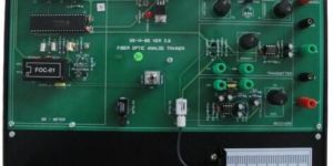
Optical communication has many advantages over the traditional electrical counterparts. It is insensitive to electromagnetic interference, it offers ground and voltage isolation between the transmitter and the receiver, it provides security from tapping and there will be no sparking at the connecting ends.
This trainer uses LEDs in visible range (660 nM) as transmitter, fast PIN-Photodiodes as receiver. A Plastic Optic Fiber (POF) is used as the channel connecting light signal from the transmitter to the receiver. Each of the transmitter and receiver are placed in a PCB mountable plastic housing. A 2.2 mm aperture is provided to hold standard 1000 micron POF. No fiber stripping is required. Microlens is a part of the housing.
exas Instrument’s TMS320C6713 DSP operating at 225 Mhz.
Embedded USBJTAG controller with plug and play drivers, USB cable included
TLV320AIC codec
2M x 32 on board SDRAM
512K bytes of on board Flash ROM
3 Expansion connectors (Memory Interface, Peripheral Interface and Host Port Interface)
On board IEEE 1149.1 JTAG connection for optional emulator debug
Four 3.5 mm audio jacks (microphone, line-in, speaker and line out)
4 user definable LEDs
4 position dip switch, user definable
+5 Volt operation only, power supply included
Si ze : 8. 25" x 4. 5" ( 210 x 115 mm) , 0. 062" t hi ck,6 layers
Compatible with Spectrum Digital’s DSK Wire Wrap Prototype Card
SOFTWARE FEATURES:
TMS320C6713 DSK specific Code Composer Studio from Tex as Instruments
Test sample code provided to reduce coding time
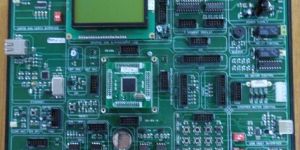
LPC1768 32 Bit ARM Cortex-M3 based processor with 512K bytes Program Flash, 64K bytes RAM
12MHz Crystal allows easy communication setup
One on board voltage regulator for generating 3.3V. Input to this will be from External +5V DC Power supply through a 9-pin DSUB connector
Reset push-button for resetting the controller
Three of the four controller UART's are made available to user for external interfaces
- UART0: General purpose RS232 terminated in a 9 pin female DSUB connector which is also used to program LPC1768 Flash memory without external Programmer
- UART1: General purpose RS485 terminated in a 3 pin male reliamate
- UART2: General purpose RS232 terminated in a 3 pin male reliamate
Interface to Controller internal ADC and DAC
16×2 alphanumeric LCD and 128×64 Graphic LCD display are provided – one of them can be used at a time
4×4 Key-Matrix
SPI interface: Flash NVROM memory circuit
Simple I2S demonstration circuit
I2C interface: RTC IC
Eight general purpose LED’s
Four-digit multiplexed 7-segment display interface
Interface circuit for external Interrupt
Interface circuit for Capture & match
Interface circuit for PWM with a monitor LED
On-board stepper motor, DC motor control, Relay interface
Interface circuit for on board Buzzer
Ethernet interface with RJ45 female connector
...more
ARM Cortex M3 Evaluation Board ALS-SDA-ARMCTXM3-01
LPC1768 32 Bit ARM Cortex-M3 based processor with 512K bytes Program Flash, 64K bytes RAM
12MHz Crystal allows easy communication setup
One on board voltage regulator for generating 3.3V. Input to this will be from External +5V DC Power supply through a 9-pin DSUB connector
Reset push-button for resetting the controller
Three of the four controller UART's are made available to user for external interfaces
- UART0: General purpose RS232 terminated in a 9 pin female DSUB connector which is also used to program LPC1768 Flash memory without external Programmer
- UART1: General purpose RS485 terminated in a 3 pin male reliamate
- UART2: General purpose RS232 terminated in a 3 pin male reliamate
Interface to Controller internal ADC and DAC
16×2 alphanumeric LCD and 128×64 Graphic LCD display are provided – one of them can be used at a time
4×4 Key-Matrix
SPI interface: Flash NVROM memory circuit
Simple I2S demonstration circuit
I2C interface: RTC IC
Eight general purpose LED’s
Four-digit multiplexed 7-segment display interface
Interface circuit for external Interrupt
Interface circuit for Capture & match
Interface circuit for PWM with a monitor LED
On-board stepper motor, DC motor control, Relay interface
Interface circuit for on board Buzzer
Ethernet interface with RJ45 female connector
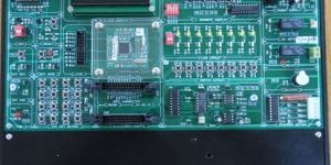
LPC1768 is ARM Cortex M3 based micro controller with 512KB flash memory and 64KB SRAM
12MHz Crystal allows easy communication setup
One on board voltage regulator for generating 3.3V. Input to this will be from External +5V DC Power supply through a 9-pin DSUB connector
One RS232 interface circuits with 9 pin DSUB connector: this is used by the Boot loader program, to program LPC1768 Flash memory without external Programmer
Piggy Back module containing LPC1768 controller
Standard JTAG connector with ARM 2×10 pin layout for programmingdebugging with ARM-JTAG
Standard 26-pin FRC connectors to connect to on-board interface or some of ALS standard External Interfaces
Reset push-button for resetting the controller
SPI Interface: 2 channel ADC IC with POT and Temperature sensor
I2C Interface: NVROM IC
On chip ADC interface circuit
Two External interrupt circuits with LED indication
LCD 16×2 alphanumeric display
On-board eight push-button switches
4x4 Key-Matrix connected to the port lines of the controller
Eight general purpose LED’s
Four-digit multiplexed 7-segment display interface
8-bit DAC interface
...more
ARM Cortex M3 Evaluation Board 02 ALS-SDA-ARMCTXM3-02
LPC1768 is ARM Cortex M3 based micro controller with 512KB flash memory and 64KB SRAM
12MHz Crystal allows easy communication setup
One on board voltage regulator for generating 3.3V. Input to this will be from External +5V DC Power supply through a 9-pin DSUB connector
One RS232 interface circuits with 9 pin DSUB connector: this is used by the Boot loader program, to program LPC1768 Flash memory without external Programmer
Piggy Back module containing LPC1768 controller
Standard JTAG connector with ARM 2×10 pin layout for programmingdebugging with ARM-JTAG
Standard 26-pin FRC connectors to connect to on-board interface or some of ALS standard External Interfaces
Reset push-button for resetting the controller
SPI Interface: 2 channel ADC IC with POT and Temperature sensor
I2C Interface: NVROM IC
On chip ADC interface circuit
Two External interrupt circuits with LED indication
LCD 16×2 alphanumeric display
On-board eight push-button switches
4x4 Key-Matrix connected to the port lines of the controller
Eight general purpose LED’s
Four-digit multiplexed 7-segment display interface
8-bit DAC interface
Modular Design: ARM9 daughter board and feature rich Motherboard.
The SM-9302, daughter board, is actually an ARM9 SBC, with on board
Uses EP-9302 ARM9 processor
Flash 8 MB
SDRAM 32 MB
Also IO and bus lines available on connector for further use
Ethernet connectivity through RJ45 connector
Dual USB host
Works on 5V, other voltages generated on board.
Thus working as an independent unit, so can be used in ARM9 based projects
4x4 Matrix keypad
16x2 Lcd
8 keys for digital ip
8 LEDS for digital op
I2C based RTC
I2C 7 Segment Display
SPI based EEPROM
Stepper Motor with driver interface
POT for giving Analog input
Temperature sensor interface
BSP provided with Lots of Examples. Example included webserver application.
20 Pin Jtag Connector
Serial port: 1 RS232, 1 RS485 port
The Cygnal Micro controller C8051F320 operating at a Frequency of 24MHz and a supply voltage of 3.3V.
Universal Serial Bus (USB) Function Controller with eight flexible endpoint pipes, integrated transceiver, and 1k FIFO RAM.
True 10-bit 200 kbps, 17-channel single-endeddifferential ADC analog multiplexer.
16k bytes of on-chip FLASH memory, 2304 bytes of on-chip RAM.
SMBusI2C, Enhanced UART, and Enhanced SPI serial interfaces implemented in hardware.
On-chip Voltage Reference and Temperature Sensor.
Four general-purpose 16-bit timers, PCA with five capturecompare modules and watchdog timer function.
On-chip voltage reference and temperature sensor.
On-chip voltage comparators (2).
2521 Port IO (5V tolerant).
32 inputs using 8-way four DIP switches. Each input of these switches has an LED indication.
32 outputs through output ports of FPGA connected to LEDs.
16x2 Alpha�Numeric LCD display with back-light through 10 PIN FRC Connectors to FPGACPLD port pins.
Six-digit 7-segment displays connected through 10 PIN FRC connector to FPGACPLD port pins .
4x4 key matrix.
10 MHz, 5 MHz, 1MHz, 500 KHz, 100 KHz - five different clock frequencies.
On-board Relay connected using 10 pin FRC to FPGACPLD port pins.
On-board Traffic Light Simulator connected to FPGACPLD port pins using 16 pin FRC.
On-board ADC connected to FPGACPLD port pins using 16 pin FRC.
On-board DAC is provided to generate different waveforms and it is connected to FPGACPLD port pins using 16 pin FRC.
On-board four level Elevator connected to FPGACPLD port pins using 16 pin FRC.
Two-pin reliamate is provided on the board to connect external DC motor and it is connected to FPGACPLD port pins using 10 pin FRC.
5-way PowerMate is provided to connect external stepper motor and it is connected to FPGACPLD port pins using 10 pin FRC.
26-PIN FRC header with Cable for connecting to ALS standard interfaces.
8 inputs using 0ne DIP switches. Each input of these switches has an LED indication.
One push button
Four sets of 20x2 female berg connector to plug the DAUGHTER BOARD
Ethernet Interface (WIZNET 7010B+ or equivalent).
16x2 alphanumeric display (LCD) with back light
On board switches and LED’s.
Circuit to test on-chip Compare, Capture, PWM and Analog Comparator.
RS232C Serial interface through on chip UART0 and UART1.
On-chip 10-bit ADC0 and ADC1 is used for 4-20mA current loop interface.
On-chip 10-bit ADC2 is used for voltage interface.
On-chip 10-bit ADC3 is used for ambient temperature measurement circuit using LM335.
Onboard interface to SPI compatible 12-bit DAC device and SD card.
Onboard interface to I2C compatible NVROM (Non Volatile Read Only Memory) and RTC (PCF8523).
A 10 pin FRC box connector for interfacing external GPS module using UART0UART1.
A 9-pin Female D-sub connector for interfacing external GSM module using UART1.
A 9-pin Male D-sub connector for interfacing RS485 interface using UART1.
USB to serial interface using UART0 and onboard USB interface IC.
CPLD is used for counter operation and generation of chip selects for onboard interfaces.
Provision for JTAG and ISP for debugging and programming the controller.
Elegant enclosure with Test Points for monitoring.
Software examples compiled using ICC-AVR compiler.
Provision to interface ALS standard external interfaces through 26 pin FRC
Power supply required – +5V DC, 1.5A.
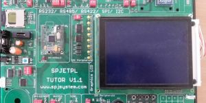
Tutor based on LPC2148 ARM 7 Controller
Speed:12Mhz default,up to 60Mhz with on chip PLL
Protocol supported
RS232
RS485
I2C
SPI
Zigbee(1no)
GPS Module(1no)
Flash -512KB,SRAM-32KB
320X240 Monochrome Graphics LCD included on board
UART for programming
UART for full UART
UART for RS485
UART for RS422
SD card interface
Onboard temperature sensor interface using LM35
8 LEDs to display I2C
4X4 Matrix keyboard
Stepper motor interface with on board motor
I2C compatible
EEPROM(64KB)
RTC with suitable battery
SPI compatible EEPROM(32KB)
Microcontroller LPC2148 provided as daughter board for easy maintenance
Buzzer
Different test points for each protocol
Software Features:
Tutorial for RS232
Tutorial for RS422
Tutorial for RS485
Tutorial for SPI
Tutorial for I2C
Tutorial for Zigbeee
Tutorial for GPS
Sample application for protocol:RS232(Serial communication)
RS422(Full duplex),RS485 (Half duplex) SPI (EEPROM) I2C(EEPROM)
Code compilation using SCARM
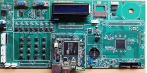
LPC2148 1632 BIT ARM7TDMI-S with 512K bytes Program Flash, 42K bytes RAM
12MHz Crystal allows easy communication setup
One on board voltage regulator for generating 3.3V. Input to this will be from External +5V DC Power supply through a 9-pin DSUB connector
One RS232 interface circuits with 9 pin DSUB connector: this is used by the Boot loader program, to program LPC2148 Flash memory without external Programmer
Piggy Back module containing LPC2148 controller
Standard JTAG connector with ARM 2×10 pin layout for programmingdebugging with ARM-JTAG
Standard 26-pin FRC connectors to connect to on-board interface or some of ALS standard External Interfaces
Reset push-button for resetting the controller
SPI Interface: 2 channel ADC IC with POT and Temperature sensor
I2C Interface: NVROM IC
On chip ADC interface circuit
Two External interrupt circuits with LED indication
LCD 16×2 alphanumeric display
On-board eight push-button switches
4x4 Key-Matrix connected to the port lines of the controller
Eight general purpose LED’s
Four-digit multiplexed 7-segment display interface
8-bit DAC interface
Stepper motor interface with direction and speed control
DC motor interface with direction and speed control
Interface circuit for on board Buzzer and Relay
A number of software examples in ‘C-language’ to illustrate the functioning of the interfaces. The software examples are compiled using an evaluation version of KEIL4 ‘C’ compiler for ARM
Compact elegant plastic enclosure
Serial RS232 cable is included
Operates off 5V DC
CPU 8086 Operating @ 5 MHz in MAX MODE with provision for 8087 co-processor
MEMORY Maximum of 128 kb on board EPROM MAXIMUM OF 64 KB ON BOARD RAM. Battery Backup option for RAM
NOTE The system is supplied with 64KB EPROM and 64 KB RAMand 8KB RAM
IO PARALLEL 48 IO lines using two 8255
IO SERIAL 0ne RS232 compatible interface
TIMER Three 16 bit counter timer using 8253
KEYBOARD External PC-AT compatible keyboard
DISPLAY 16 characters 2 line JUMBO LCD display
BUS SIGNALS All Address, Data and Control signals are terminated in 50 pin berg stick for user expansion
PIC PROGRAMMABLE INTERRUPT CONTROLLER USING 8259
MONITOR SOFTWARE 64KB of system monitor, which allows the user to enter, verify, debug or execute the program either from the on-board PC keyboard and display or through serial mode. On-line assembler using PC keyboard and LCD display
CPU 8086 Operating @ 5MHz in MAX mode with provision for 8087 Co-processor
MEMORY Maximum of 128KB on board EPROM. Maximum 64KB of on board RAM. Battery Backup option for RAM
IO PARALLEL 48 IO lines using two 8255
IO SERIAL 0ne RS232 compatible interface
TIMER Three 16 bit countertimer using 8253
KEYBOARD Consisting of 28 numbers of computer grade keys
DISPLAY Eight numbers of seven segment displays
BUS SIGNALS All Address, Data and Control signals are terminated in 50 pin berg stick for user expansion
PIC Programmable Interrupt controller using 8259
MONITOR SOFTWARE 64KB of powerful user friendly monitor software with keyboard and serial modes