Memsstar’s XERIC dry release etch process module is available using vapor Hydrogen Fluoride (HF) andXenon DiFluoride (XeF2) chemistries.
Offers solutions for commercial R&D through to full-scale high volume manufacturing.
XERIC Etch process module offers the strongest approach to effectively releasing MEMS structures from the sacrificial layer, while eliminating the problems associated with alternative approaches, including stiction, incompatible and poorly controlled wet chemistries, poor control and monitoring of stagnant gas systems, and multiplicity of unit
INFICON market-leading thin film deposition controllers, monitors and QCM measurement instruments control deposition rate and thickness of the most complex processes with unsurpassed measurement speed and precision. Enhanced software and logic I/O features allow the our thin film deposition controllers.
INFICON market-leading thin film deposition controllers, monitors and QCM measurement instruments control deposition rate and thickness of the most complex processes with unsurpassed measurement speed and precision. Enhanced software and logic I/O features allow the our thin film deposition controllers.
PL-004-THERM
Microtech
Plasma-Therm’s 790™ platform is the latest in the 790™ Series of cost-efficient systems. Has been field demonstrated to have low maintenance requirements and is easily operated in R&D through high production environments.
PL-004-THERM
Microtech
Plasma-Therm’s 790™ platform is the latest in the 790™ Series of cost-efficient systems. Has been field demonstrated to have low maintenance requirements and is easily operated in R&D through high production environments.
Memsstar’s Orbis dry release etch process tools are available using vapor Hydrogen Fluoride (HF) andXenon DiFluoride (XeF2) chemistries.
Available in variants Alpha, 1000 and 3000.
The new generation of ORBIS platforms enable the most advanced processing capability from research, to commercial R&D through to high-volume manufacturing.
The ORBIS platform approach delivers many benefits to our customers, such as:
1. Upgrade paths from R&D through to full-scale production
2. Cost-effective solutions—lab or fab
3. Seamless process transfer—from lab to fab
4. Low cost of ownership
Measuring Microscope that has been designed based on an optical type focal point detection system. Adopting precise focus indicator, it's possible to measure height, depth, steps, etc. with observing the surface of measuring point, by simply coinciding the halves of an index graticule. Since there are no concern for physical damages such as distortion, blow or nicks to a specimen because of non-contact system, HISOMET is optimum for measuring electronic components such as ICs or high-precision processing parts.
Measuring Microscope that has been designed based on an optical type focal point detection system. Adopting precise focus indicator, it's possible to measure height, depth, steps, etc. with observing the surface of measuring point, by simply coinciding the halves of an index graticule. Since there are no concern for physical damages such as distortion, blow or nicks to a specimen because of non-contact system, HISOMET is optimum for measuring electronic components such as ICs or high-precision processing parts.
FEATURES
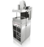
Wafer Size: up to 4” dia Economical, Compact & Hi-Level Performance Viewing fused image of two alignment marks in the field of view. Integrator lens for exposure. LED illuminator
APPLICATIONS
(Micromachine development in R&D center and university) Acuator, Pressure Sensor, Acceleration Sensor, Power Device, etc. Exposure for Flip Chip/BGA/CSP. Exposure for Optical/High Speed Communication Components.
FEATURES
Wafer Size: up to 4” dia Economical, Compact & Hi-Level Performance Viewing fused image of two alignment marks in the field of view. Integrator lens for exposure. LED illuminator
APPLICATIONS
(Micromachine development in R&D center and university) Acuator, Pressure Sensor, Acceleration Sensor, Power Device, etc. Exposure for Flip Chip/BGA/CSP. Exposure for Optical/High Speed Communication Components.
INFICON market-leading thin film deposition controllers, monitors and QCM measurement instruments control deposition rate and thickness of the most complex processes with unsurpassed measurement speed and precision. Enhanced software and logic I/O features allow the our thin film deposition controllers.
INFICON market-leading thin film deposition controllers, monitors and QCM measurement instruments control deposition rate and thickness of the most complex processes with unsurpassed measurement speed and precision. Enhanced software and logic I/O features allow the our thin film deposition controllers.
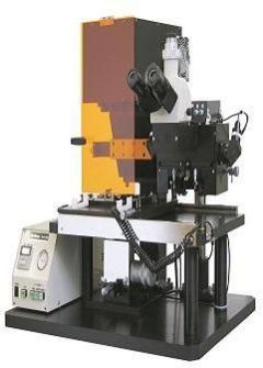
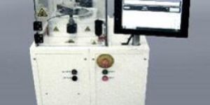
DCM-40/60 are unique microscope systems superimposing top and bottom patterns of specimen (wafer) in the view field of microscope, then comparing shift to measure the shift length by measuring system. Since the objective lenses installed at top and bottom are 5 types, ranging from 50X to 1000X in total magnification, various specimens can be observed.
DCM-40/60 are unique microscope systems superimposing top and bottom patterns of specimen (wafer) in the view field of microscope, then comparing shift to measure the shift length by measuring system. Since the objective lenses installed at top and bottom are 5 types, ranging from 50X to 1000X in total magnification, various specimens can be observed.
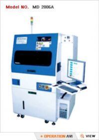
All the works necessary for decap are realized through Auto Decaper The automated robot decapsulation system that has been developed first in the world The functions of milling, etching, heating, acetone cleaning, drying, ultrasonic cleaning and vision inspection available.
Function & Features
• All the works necessary for decap are realized through Auto Decaper • The automated robot decapsulation system that has been developed first in the world • The functions of milling, etching, heating, acetone cleaning, drying, ultrasonic cleaning and vision inspection available • Protecting workers from harmful chemicals • Minimizing damage etching of copper in the case of copper wired IC • Minimizing the damage on the ball or the tape at the bottom of a package • Fast, safe, and efficient decapsulation • Protecting workers and equipment through the built-in exhaust system • The functions of checking decap results through enlarged clear images, saving images, and printing images available • Dual heating (MIS-specialized technology) • More precise, faster, and safer decap possible • Easy control through convenient GUI • Repetitions made simple using recipe files • Consumable gaskets are unnecessary and very small amount of etching chemical is used • Expanded decap possibility for various sizes and patterns of packages • Minimal maintenance and repair costs, and long lifecycles
AURIX dry, vapor-phase SAM coatings offer major advantages over traditional wet chemical coatings. In particular, the vacuum deposition environment eliminates issues of moisture variation, crucial in creating repeatable and robust surface coatings.
Precision-tuned processes, with patented control, reduce the amounts of chemicals used, offer superior surface properties and improved surface energy control.
With AURIX, SAM coatings can be created immediately following the release etching process. This enables the MEMS structure to be treated without breaking process-vacuum, maximizing yield.
Our results have consistently demonstrated superior film characteristics, with durability, coverage and yield, when compared with wet chemical approaches.
Aremco’s Accu-Coat™ Screen Printers offer the finest technology for precision screening of electronic components and other materials up to 24”. Accu-Coat™ printers represent the best price/performance ratio throughout the industry, providing the most accurate, reliable and cost effective solution for your screen printing needs.
Aremco’s Accu-Coat™ Screen Printers offer the finest technology for precision screening of electronic components and other materials up to 24”. Accu-Coat™ printers represent the best price/performance ratio throughout the industry, providing the most accurate, reliable and cost effective solution for your screen printing needs.
Secondary Business TypeManufacturer / Exporters / Wholesale Suppliers
Opening Hours
SUN : Closed
MON : 9:30 AM - 6:30 PM
TUE : 9:30 AM - 6:30 PM
WED : 9:30 AM - 6:30 PM
THU : 9:30 AM - 6:30 PM
FRI : 9:30 AM - 6:30 PM
SAT : 9:30 AM - 6:30 PM
WELCOME TO GLOBAL MARKETING SERVICES, INDIA World has turned flat – thanks to the multifold growth in Satellite communication, internet, desktop computing,and mobile telephony. Innovation in semiconductor technology has been one of the key drivers for this growth. With its rich base of research institutions and various electronics manufacturing companies, India, has emerged to be a hub of innovation in MEMS, Solar and Microelectronics technologies. Sourcing the right semiconductor equipment and manufacturing processes has always been a complex process. Companies find it a challenge to find the right partner who provides technology consulting and efficient product procurement. Global Marketing Services, has been playing a major role in addressing this bottleneck. GMS brings along vast industrial experience and expertise. Over the years GMS, has established successful relationship with some of the leading solution providers and manufacturers of semicon technology in processes and device assembly solutions. GMS adds value to its customers through consultancy, procurement and after sales support.