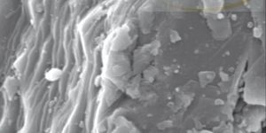
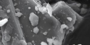
vanadium aluminum carbide v2alc max phase powder v2alc is a member of vdw max layered material system. similar to graphite and mos2, the max phases are layered and have the general formula: mn+1axn, (max) where n = 1 to 3, m is an early transition metal, a is an non-metal elements and x is either carbon and/or nitrogen. in this particular case, m=v, a=al, and x=c with n=2.world’s first electronic and optical grade commercial layered maxene phase v2alc materials: v2alc max phase has been synthesized at our facilities using large reactor chemical vapor deposition to yield world’s highest purity (99.999% or higher guaranteed) and layered max phases. the max phases are electrically and thermally conductive due to their metallic-like nature of bonding. they are excellent for research quality materials as 2d metals, battery applications, supermetallicity, thermal physics, or as precursors for mxene production. they have been also subject to research for isolating single layer al (alumine) owing to isolated al layers (see atomistic views). v2alc product consists of microsized layered crystals that measure from 2 microns to 100 microns in size (see sem images below). each order contains large volume 1250 mg of high purity and layered v2alc maxenes sealed under inert ar gas. the product has been perfected in the last years to reach guaranteed 2:1:2 v:al:c ratios and exhibit extraordinary environmental stability. xrd peaks are rather sharp and sem images clearly exhibit layered nature of the flakes. each crystallite can be exfoliated either using conventional tape exfoliation or alternatively liquid phase exfoliation technique.if you have specific type of new maxene and mxene phases in mind please contact us. our research and development team will be happy to design, synthesize, and provide new types of materials on demand.
vanadium aluminum carbide v2alc max phase powder v2alc is a member of vdw max layered material system. similar to graphite and mos2, the max phases are layered and have the general formula: mn+1axn, (max) where n = 1 to 3, m is an early transition metal, a is an non-metal elements and x is either carbon and/or nitrogen. in this particular case, m=v, a=al, and x=c with n=2.world’s first electronic and optical grade commercial layered maxene phase v2alc materials: v2alc max phase has been synthesized at our facilities using large reactor chemical vapor deposition to yield world’s highest purity (99.999% or higher guaranteed) and layered max phases. the max phases are electrically and thermally conductive due to their metallic-like nature of bonding. they are excellent for research quality materials as 2d metals, battery applications, supermetallicity, thermal physics, or as precursors for mxene production. they have been also subject to research for isolating single layer al (alumine) owing to isolated al layers (see atomistic views). v2alc product consists of microsized layered crystals that measure from 2 microns to 100 microns in size (see sem images below). each order contains large volume 1250 mg of high purity and layered v2alc maxenes sealed under inert ar gas. the product has been perfected in the last years to reach guaranteed 2:1:2 v:al:c ratios and exhibit extraordinary environmental stability. xrd peaks are rather sharp and sem images clearly exhibit layered nature of the flakes. each crystallite can be exfoliated either using conventional tape exfoliation or alternatively liquid phase exfoliation technique.if you have specific type of new maxene and mxene phases in mind please contact us. our research and development team will be happy to design, synthesize, and provide new types of materials on demand.
Titanium silicon carbide Ti3SiC2 is a member of vdW MAX layered material system. Similar to graphite and MoS2, the MAX phases are layered and have the general formula: Mn+1AXn, (MAX) where n = 1 to 3, M is an early transition metal, A is a non-metal element and X is either carbon and/or nitrogen. In this particular case, M=Ti, A=Si, and X=C with n=3.
Worlds first electronic and optical grade commercial layered MAXene phase Ti3SiC2 materials: Ti3SiC2 MAX phase has been synthesized at our facilities using large reactor chemical vapor deposition to yield Worlds highest purity (99.999% or higher guaranteed) and layered MAX phases.
The MAX phases are electrically and thermally conductive due to their metallic-like nature of bonding. They are excellent for research quality materials as 2D metals, battery applications, supermetallicity, thermal physics, or as precursors for MXene production. They have been also subject to research for isolating single layer Silicon (silicene) or Al (alumine) owing to isolated Si and Al between layers (see atomistic views).
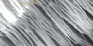
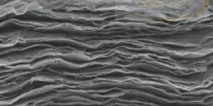
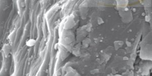
Ti3SiC2 product consists of microsized layered crystals that measure from 1 micron to 100 microns in size (see SEM images below).
Each order contains 100 grams of high purity and layered Ti3SiC2 MAXenes sealed under inert Ar gas.
The product has been perfected in the last years to reach guaranteed 3:1:2 Ti:Si:C ratios and exhibit extraordinary environmental stability. XRD peaks are rather sharp and SEM images clearly exhibit layered nature of the flakes. Each crystallite can be exfoliated either using conventional tape exfoliation or alternatively liquid phase exfoliation technique.
If you have a specific type of new MAXene and MXene phases in mind please contact us. Our research and development team will be happy to design, synthesize, and provide with new types of materials on demand.
Titanium silicon carbide Ti3SiC2 is a member of vdW MAX layered material system. Similar to graphite and MoS2, the MAX phases are layered and have the general formula: Mn+1AXn, (MAX) where n = 1 to 3, M is an early transition metal, A is a non-metal element and X is either carbon and/or nitrogen. In this particular case, M=Ti, A=Si, and X=C with n=3.
Worlds first electronic and optical grade commercial layered MAXene phase Ti3SiC2 materials: Ti3SiC2 MAX phase has been synthesized at our facilities using large reactor chemical vapor deposition to yield Worlds highest purity (99.999% or higher guaranteed) and layered MAX phases.
The MAX phases are electrically and thermally conductive due to their metallic-like nature of bonding. They are excellent for research quality materials as 2D metals, battery applications, supermetallicity, thermal physics, or as precursors for MXene production. They have been also subject to research for isolating single layer Silicon (silicene) or Al (alumine) owing to isolated Si and Al between layers (see atomistic views).
Ti3SiC2 product consists of microsized layered crystals that measure from 1 micron to 100 microns in size (see SEM images below).
Each order contains 100 grams of high purity and layered Ti3SiC2 MAXenes sealed under inert Ar gas.
The product has been perfected in the last years to reach guaranteed 3:1:2 Ti:Si:C ratios and exhibit extraordinary environmental stability. XRD peaks are rather sharp and SEM images clearly exhibit layered nature of the flakes. Each crystallite can be exfoliated either using conventional tape exfoliation or alternatively liquid phase exfoliation technique.
If you have a specific type of new MAXene and MXene phases in mind please contact us. Our research and development team will be happy to design, synthesize, and provide with new types of materials on demand.
Ti3AlC2 is a member of vdW MAX layered material system. Similar to graphite and MoS2, the MAX phases are layered and have the general formula: Mn+1AXn, (MAX) where n = 1 to 3, M is an early transition metal, A is a non-metal elements and X is either carbon and/or nitrogen. In this particular case, M=Ti, A=Al, and X=C with n=3.
World’s first electronic and optical grade commercial layered MAXene phase Ti3AlC2 materials:
Ti3AlC2 MAX phase has been synthesized at our facilities using large reactor chemical vapor deposition to yield World’s highest purity (99.999% or higher guaranteed) and layered MAX phases.
The MAX phases are electrically and thermally conductive due to their metallic-like nature of bonding.
They are excellent for research quality materials as 2D metals, battery applications, supermetallicity, thermal physics, or as precursors for MXene production.
They have been also subject to research for isolating single layer Silicon (silicene) or Al (alumine) owing to isolated Si and Al between layers.
Ti3AlC2 product consists of microsized layered crystals that measure from 1 micron to 100 microns in size.
Each order contains a very large volume of 5000 mg of high purity and layered Ti3AlC2 MAXenes sealed under inert Ar gas.
The product has been perfected in the last years to reach guaranteed 3:1:2 Ti:Al:C ratios and exhibit extraordinary environmental stability. Each crystallite can be exfoliated either using conventional tape exfoliation or alternatively liquid phase exfoliation technique.
Ti3AlC2 is a member of vdW MAX layered material system. Similar to graphite and MoS2, the MAX phases are layered and have the general formula: Mn+1AXn, (MAX) where n = 1 to 3, M is an early transition metal, A is a non-metal elements and X is either carbon and/or nitrogen. In this particular case, M=Ti, A=Al, and X=C with n=3.
World’s first electronic and optical grade commercial layered MAXene phase Ti3AlC2 materials:
Ti3AlC2 MAX phase has been synthesized at our facilities using large reactor chemical vapor deposition to yield World’s highest purity (99.999% or higher guaranteed) and layered MAX phases.
The MAX phases are electrically and thermally conductive due to their metallic-like nature of bonding.
They are excellent for research quality materials as 2D metals, battery applications, supermetallicity, thermal physics, or as precursors for MXene production.
They have been also subject to research for isolating single layer Silicon (silicene) or Al (alumine) owing to isolated Si and Al between layers.
Ti3AlC2 product consists of microsized layered crystals that measure from 1 micron to 100 microns in size.
Each order contains a very large volume of 5000 mg of high purity and layered Ti3AlC2 MAXenes sealed under inert Ar gas.
The product has been perfected in the last years to reach guaranteed 3:1:2 Ti:Al:C ratios and exhibit extraordinary environmental stability. Each crystallite can be exfoliated either using conventional tape exfoliation or alternatively liquid phase exfoliation technique.
Ti2AlN is a member of vdW MAX layered material system. Similar to graphite and MoS2, the MAX phases are layered and have the general formula: Mn+1AXn, (MAX) where n = 1 to 3, M is an early transition metal, A is an non-metal elements and X is either carbon and/or nitrogen. In this particular case, M=Ti, A=Al, and X=N with n=2.
World’s first electronic and optical grade commercial layered MAXene phase Ti2AlN materials: Ti2AlN MAX phase has been synthesized at our facilities using large reactor chemical vapor deposition to yield World’s highest purity (99.999% or higher guaranteed) and layered MAX phases.
The MAX phases are electrically and thermally conductive due to their metallic-like nature of bonding. They are excellent for research quality materials as 2D metals, battery applications, supermetallicity, thermal physics, or as precursors for MXene production. They have been also subject to research for isolating single layer Silicon (silicene) or Al (alumine) owing to isolated Si and Al between layers.
Ti2AlN product consists of microsized layered crystals that measure from 2 microns to 100 microns in size.
Each order contains large volume 1000 mg of high purity and layered Ti2AlN MAXenes sealed under inert Ar gas.
The product has been perfected in the last years to reach guaranteed 2:1:2 Ti:Al:N ratios and exhibit an extraordinary environmental stability. XRD peaks are rather sharp and SEM images clearly exhibit layered nature of the flakes.
Each crystallite can be exfoliated either using conventional tape exfoliation or alternatively liquid phase exfoliation technique.
Ti2AlN is a member of vdW MAX layered material system. Similar to graphite and MoS2, the MAX phases are layered and have the general formula: Mn+1AXn, (MAX) where n = 1 to 3, M is an early transition metal, A is an non-metal elements and X is either carbon and/or nitrogen. In this particular case, M=Ti, A=Al, and X=N with n=2.
World’s first electronic and optical grade commercial layered MAXene phase Ti2AlN materials: Ti2AlN MAX phase has been synthesized at our facilities using large reactor chemical vapor deposition to yield World’s highest purity (99.999% or higher guaranteed) and layered MAX phases.
The MAX phases are electrically and thermally conductive due to their metallic-like nature of bonding. They are excellent for research quality materials as 2D metals, battery applications, supermetallicity, thermal physics, or as precursors for MXene production. They have been also subject to research for isolating single layer Silicon (silicene) or Al (alumine) owing to isolated Si and Al between layers.
Ti2AlN product consists of microsized layered crystals that measure from 2 microns to 100 microns in size.
Each order contains large volume 1000 mg of high purity and layered Ti2AlN MAXenes sealed under inert Ar gas.
The product has been perfected in the last years to reach guaranteed 2:1:2 Ti:Al:N ratios and exhibit an extraordinary environmental stability. XRD peaks are rather sharp and SEM images clearly exhibit layered nature of the flakes.
Each crystallite can be exfoliated either using conventional tape exfoliation or alternatively liquid phase exfoliation technique.
Ta4AlC3 is a member of vdW MAX layered material system. Similar to graphite and MoS2, the MAX phases are layered and have the general formula: Mn+1AXn, (MAX) where n = 1 to 3, M is an early transition metal, A is a non-metal element and X is either carbon and/or nitrogen. In this particular case, M=Ta, A=Al, and X=C with n=3.
World’s first electronic and optical grade commercial layered MAXene phase Ta4AlC3 materials: Ta4AlC3 MAX phase has been synthesized at our facilities using large reactor chemical vapor deposition to yield World’s highest purity (99.999% or higher guaranteed) and layered MAX phases.
The MAX phases are electrically and thermally conductive due to their metallic-like nature of bonding. They are excellent for research quality materials as 2D metals, battery applications, supermetallicity, thermal physics, or as precursors for MXene production.
Ta4AlC3 product consists of microsized layered crystals that measure from 1 micron to 100 microns in size.
Each order contains 2000 mg of high purity and layered Ta4AlC3 MAXenes sealed under inert Ar gas.
The product has been perfected in the last years to reach guaranteed 4:1:3 Ta:Al:C ratios and exhibit extraordinary environmental stability. Each crystallite can be exfoliated either using conventional tape exfoliation or alternatively liquid phase exfoliation technique.
Ta4AlC3 is a member of vdW MAX layered material system. Similar to graphite and MoS2, the MAX phases are layered and have the general formula: Mn+1AXn, (MAX) where n = 1 to 3, M is an early transition metal, A is a non-metal element and X is either carbon and/or nitrogen. In this particular case, M=Ta, A=Al, and X=C with n=3.
World’s first electronic and optical grade commercial layered MAXene phase Ta4AlC3 materials: Ta4AlC3 MAX phase has been synthesized at our facilities using large reactor chemical vapor deposition to yield World’s highest purity (99.999% or higher guaranteed) and layered MAX phases.
The MAX phases are electrically and thermally conductive due to their metallic-like nature of bonding. They are excellent for research quality materials as 2D metals, battery applications, supermetallicity, thermal physics, or as precursors for MXene production.
Ta4AlC3 product consists of microsized layered crystals that measure from 1 micron to 100 microns in size.
Each order contains 2000 mg of high purity and layered Ta4AlC3 MAXenes sealed under inert Ar gas.
The product has been perfected in the last years to reach guaranteed 4:1:3 Ta:Al:C ratios and exhibit extraordinary environmental stability. Each crystallite can be exfoliated either using conventional tape exfoliation or alternatively liquid phase exfoliation technique.
nb4alc3 is a member of the vdw max layered material system. similar to graphite and mos2, the max phases are layered and have the general formula: mn+1axn, (max) where n = 1 to 3, m is an early transition metal, a is a non-metal element and x is either carbon and/or nitrogen. in this particular case, m=nb, a=al, and x=c with n=3.
world’s first electronic and optical grade commercial layered maxene phase nb4alc3 materials: nb4alc3 max phase has been synthesized at our facilities using large reactor chemical vapor deposition to yield world’s highest purity (99.999% or higher guaranteed) and layered max phases.
the max phases are electrically and thermally conductive due to their metallic-like nature of bonding. they are excellent for research quality materials as 2d metals, battery applications, supermetallicity, thermal physics, or as precursors for mxene production.
nb4alc3 product consists of microsized layered crystals that measure from 1 micron to 100 microns in size (see sem images below).
each order contains 10 gm of high purity and layered nb4alc3 maxenes sealed under inert ar gas.
the product has been perfected in the last years to reach guaranteed 4:1:3 nb:al:c ratios and exhibit extraordinary environmental stability. each crystallite can be exfoliated either using conventional tape exfoliation or alternatively liquid phase exfoliation technique.
nb4alc3 is a member of the vdw max layered material system. similar to graphite and mos2, the max phases are layered and have the general formula: mn+1axn, (max) where n = 1 to 3, m is an early transition metal, a is a non-metal element and x is either carbon and/or nitrogen. in this particular case, m=nb, a=al, and x=c with n=3.
world’s first electronic and optical grade commercial layered maxene phase nb4alc3 materials: nb4alc3 max phase has been synthesized at our facilities using large reactor chemical vapor deposition to yield world’s highest purity (99.999% or higher guaranteed) and layered max phases.
the max phases are electrically and thermally conductive due to their metallic-like nature of bonding. they are excellent for research quality materials as 2d metals, battery applications, supermetallicity, thermal physics, or as precursors for mxene production.
nb4alc3 product consists of microsized layered crystals that measure from 1 micron to 100 microns in size (see sem images below).
each order contains 10 gm of high purity and layered nb4alc3 maxenes sealed under inert ar gas.
the product has been perfected in the last years to reach guaranteed 4:1:3 nb:al:c ratios and exhibit extraordinary environmental stability. each crystallite can be exfoliated either using conventional tape exfoliation or alternatively liquid phase exfoliation technique.
nb2alc is a member of vdw max layered material system. similar to graphite and mos2, the max phases are layered and have the general formula: mn+1axn, (max) where n = 1 to 3, m is an early transition metal, a is an non-metal elements and x is either carbon and/or nitrogen. in this particular case, m=nb, a=al, and x=c with n=1.
world's first electronic and optical grade commercial layered maxene phase nb2alc materials: nb2alc max phase has been synthesized at our facilities using large reactor chemical vapor deposition to yield world's highest purity (99.999% or higher guaranteed) and layered max phases.
the max phases are electrically and thermally conductive due to their metallic-like nature of bonding. they are excellent for research quality materials as 2d metals, battery applications, supermetallicity, thermal physics, or as precursors for mxene production.
nb2alc product consists of microsized layered crystals that measure from 1 micron to 100 microns in size (see sem images below).
each order contains 10gm of high purity and layered nb2alc maxenes sealed under inert ar gas.
the product has been perfected in the last years to reach guaranteed 2:1:1 nb:al:c ratios and exhibit an extraordinary environmental stability. each crystallite can be exfoliated either using conventional tape exfoliation or alternatively liquid phase exfoliation technique.
nb2alc is a member of vdw max layered material system. similar to graphite and mos2, the max phases are layered and have the general formula: mn+1axn, (max) where n = 1 to 3, m is an early transition metal, a is an non-metal elements and x is either carbon and/or nitrogen. in this particular case, m=nb, a=al, and x=c with n=1.
world's first electronic and optical grade commercial layered maxene phase nb2alc materials: nb2alc max phase has been synthesized at our facilities using large reactor chemical vapor deposition to yield world's highest purity (99.999% or higher guaranteed) and layered max phases.
the max phases are electrically and thermally conductive due to their metallic-like nature of bonding. they are excellent for research quality materials as 2d metals, battery applications, supermetallicity, thermal physics, or as precursors for mxene production.
nb2alc product consists of microsized layered crystals that measure from 1 micron to 100 microns in size (see sem images below).
each order contains 10gm of high purity and layered nb2alc maxenes sealed under inert ar gas.
the product has been perfected in the last years to reach guaranteed 2:1:1 nb:al:c ratios and exhibit an extraordinary environmental stability. each crystallite can be exfoliated either using conventional tape exfoliation or alternatively liquid phase exfoliation technique.
ags138n6 = formvar on 3mm 75 mesh ni grids
ags138n1 = formvar on 3mm 100 mesh ni grids
ags138n = formvar on 3mm 200 mesh ni grids
ags138n3 = formvar on 3mm 300 mesh ni grids
ags138n4 = formvar on 3mm 400 mesh ni grids
ags138nf1 = formvar on 3mm f1 finder ni grids
ags138nh7 = formvar on 3mm h7 finder ni grids
formvar coated grids without a carbon layer are suitable for tem applications up to 100kv. the films are available on grids made of copper, nickel or gold.
supplied as 25 grids in a grid box.
formvar support films can be applied to other grid sizes, material or type. further details available on request.
ags138n6 = formvar on 3mm 75 mesh ni grids
ags138n1 = formvar on 3mm 100 mesh ni grids
ags138n = formvar on 3mm 200 mesh ni grids
ags138n3 = formvar on 3mm 300 mesh ni grids
ags138n4 = formvar on 3mm 400 mesh ni grids
ags138nf1 = formvar on 3mm f1 finder ni grids
ags138nh7 = formvar on 3mm h7 finder ni grids
formvar coated grids without a carbon layer are suitable for tem applications up to 100kv. the films are available on grids made of copper, nickel or gold.
supplied as 25 grids in a grid box.
formvar support films can be applied to other grid sizes, material or type. further details available on request.
Number Of Flower : Formvar film on Nickel TEM Grids
ags138a1 = formvar on 3mm 100 mesh au grids
ags138a = formvar on 3mm 200 mesh au grids
ags138a3 = formvar on 3mm 300 mesh au grids
ags138a4 = formvar on 3mm 400 mesh au grids
ags138a5 = formvar on 2mm x 1mm au slot grids
ags138af1 = formvar on 3mm f1 finder au grids
ags138ah7 = formvar on 3mm h7 finder au grids
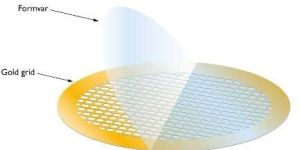
formvar coated grids without a carbon layer are suitable for tem applications up to 100kv. The films are available on grids made of copper, nickel or gold.
supplied as 25 grids in a grid box.
gold
formvar support films can be applied to other grid sizes, material or type. Further details available on request.
ags138a1 = formvar on 3mm 100 mesh au grids
ags138a = formvar on 3mm 200 mesh au grids
ags138a3 = formvar on 3mm 300 mesh au grids
ags138a4 = formvar on 3mm 400 mesh au grids
ags138a5 = formvar on 2mm x 1mm au slot grids
ags138af1 = formvar on 3mm f1 finder au grids
ags138ah7 = formvar on 3mm h7 finder au grids
formvar coated grids without a carbon layer are suitable for tem applications up to 100kv. The films are available on grids made of copper, nickel or gold.
supplied as 25 grids in a grid box.
gold
formvar support films can be applied to other grid sizes, material or type. Further details available on request.
ags138-6 = formvar on 3mm 75 mesh cu grids
ags138-1 = formvar on 3mm 100 mesh cu grids
ags138 = formvar on 3mm 200 mesh cu grids
ags138-3 = formvar on 3mm 300 mesh cu grids
ags138-4 = formvar on 3mm 400 mesh cu grids
ags138-f1 = formvar on 3mm f1 finder cu grids
ags138-h7 = formvar on 3mm h7 finder cu grids
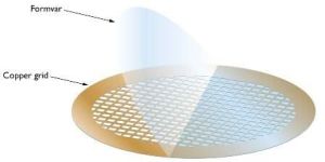
formvarâ® coated grids without a carbon layer are suitable for tem applications up to 100kv. The films are available on copper grids. Nickel and gold grids are also available.
supplied as 25 grids in a grid box.
ags138-6 = formvar on 3mm 75 mesh cu grids
ags138-1 = formvar on 3mm 100 mesh cu grids
ags138 = formvar on 3mm 200 mesh cu grids
ags138-3 = formvar on 3mm 300 mesh cu grids
ags138-4 = formvar on 3mm 400 mesh cu grids
ags138-f1 = formvar on 3mm f1 finder cu grids
ags138-h7 = formvar on 3mm h7 finder cu grids
formvarâ® coated grids without a carbon layer are suitable for tem applications up to 100kv. The films are available on copper grids. Nickel and gold grids are also available.
supplied as 25 grids in a grid box.
Number Of FlowerCarbon Films On Nickel Grids For TEM
ConditionNew
Brand NameAgar Scientific UK & TedPella USA
ApplicationLaboratory,Research
MaterialNickel,Carbon
GradeIndustrial Grade
Number Of FlowerCarbon Film On TEM Grid
ConditionNew
ShapeRound
Brand NameAgar Scientific UK & TedPella USA
ags160n = carbon films on 200 mesh nickel grids
ags160n3 = carbon films on 300 mesh nickel grids
ags160n4 = carbon films on 400 mesh nickel grids
ags160nf1 = carbon films on f1 finder grid nickel
ags160nh2 = carbon films on h2 finder grid nickel
ags160nh7 = carbon films on h7 finder grid nickel
thin and highly transparent to electrons.
supplied as packs of 25 or 50 grids in a grid box.
carbon support films can be applied to other grid sizes, material or type
.
ags160n = carbon films on 200 mesh nickel grids
ags160n3 = carbon films on 300 mesh nickel grids
ags160n4 = carbon films on 400 mesh nickel grids
ags160nf1 = carbon films on f1 finder grid nickel
ags160nh2 = carbon films on h2 finder grid nickel
ags160nh7 = carbon films on h7 finder grid nickel
thin and highly transparent to electrons.
supplied as packs of 25 or 50 grids in a grid box.
carbon support films can be applied to other grid sizes, material or type
.
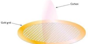
Number Of Flower : Carbon Films On Nickel Grids For TEM
AGS160A = Carbon Films on 200 Mesh Gold Grids
AGS160A-3 = Carbon Films on 300 Mesh Gold Grids
AGS160A-4 = Carbon Films on 400 Mesh Gold Grids
AGS160A-F1 = Carbon Films on F1 Finder Grid Gold
AGS160A-H2 = Carbon Films on H2 Finder Grid Gold
AGS160A-H7 = Carbon Films on H7 Finder Grid Gold
Thin and highly transparent to electrons
Offering fine grain and low contrast
Supplied as packs of 25 or 50 grids in a grid box.
Applied to other grid sizes, material or type
AGS160A = Carbon Films on 200 Mesh Gold Grids
AGS160A-3 = Carbon Films on 300 Mesh Gold Grids
AGS160A-4 = Carbon Films on 400 Mesh Gold Grids
AGS160A-F1 = Carbon Films on F1 Finder Grid Gold
AGS160A-H2 = Carbon Films on H2 Finder Grid Gold
AGS160A-H7 = Carbon Films on H7 Finder Grid Gold
Thin and highly transparent to electrons
Offering fine grain and low contrast
Supplied as packs of 25 or 50 grids in a grid box.
Applied to other grid sizes, material or type
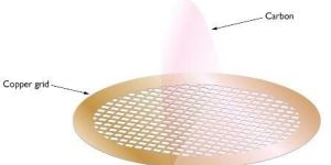
ags160 = carbon films on 200 mesh copper grids
ags160-3 = carbon films on 300 mesh copper grids
ags160-4 = carbon films on 400 mesh copper grids
ags160-f1 = carbon films on f1 finder grid copper
ags160-h2 = carbon films on h2 finder grid copper
ags160-h7 = carbon films on h7 finder grid copper
thin and highly transparent to electrons
carbon coating is 28-30nm
supplied as packs of 25 or 50 grids in a grid box.
applied to other grid sizes, material or type
ags160 = carbon films on 200 mesh copper grids
ags160-3 = carbon films on 300 mesh copper grids
ags160-4 = carbon films on 400 mesh copper grids
ags160-f1 = carbon films on f1 finder grid copper
ags160-h2 = carbon films on h2 finder grid copper
ags160-h7 = carbon films on h7 finder grid copper
thin and highly transparent to electrons
carbon coating is 28-30nm
supplied as packs of 25 or 50 grids in a grid box.
applied to other grid sizes, material or type
Secondary Business TypeExporters / Wholesale Suppliers
Year of Establishment2017
No. of Employees6 - 20
Annual TurnoverBelow Rs. 0.5 Crore Approx.
Ownership TypePartnership
GSTIN Number06ABQFA1141D1ZW
Opening Hours
SUN : Closed
MON : 9:30 AM - 6:30 PM
TUE : 9:30 AM - 6:30 PM
WED : 9:30 AM - 6:30 PM
THU : 9:30 AM - 6:30 PM
FRI : 9:30 AM - 6:30 PM
SAT : 9:30 AM - 6:30 PM
AMC is an ISO 9001 certified worldwide manufacturer and supplier of nanoparticles, nanopowders, micron powders, and CNTs (carbon nanotubes) in small quantities for research and in bulk order for industry groups. Our expertise in the properties, applications, and various manufacturing processes of advanced and engineered materials allows us to meet the needs of our customers. AMC Materials is a high-tech enterprise involved in advanced nanomaterials development and production. Our goal is to provide high-quality nanomaterial products, services, or technical proposals.




 Reviews & Ratings
 Write a Review


 Post Free Ad